
Exploring Innovative MEMS Vapor Cell Fabrication with Ultrafast Laser Welding
The world of micro-electro-mechanical systems (MEMS) vapor cell technology has witnessed some truly innovative breakthroughs over the past years. In particular, the use of ultrafast laser welding is emerging as a promising alternative to the traditional anodic bonding process. This method not only addresses some of the tricky parts and confusing bits inherent in conventional techniques, but also paves the way for better performance and reliability in quantum sensors and atomic magnetometers.
In this opinion editorial, we take a closer look at the advantages and challenges of ultrafast laser welding when used for sealing MEMS alkali metal vapor cells – a topic that has stirred plenty of discussion in the industrial manufacturing and sensor communities. We hope to offer insights into how this technology can be understood and potentially adopted by small business manufacturers, industrial players in the automotive and electric vehicle sectors, and even research labs pushing the envelope in quantum sensing.
Understanding the Evolution of MEMS Vapor Cell Sealing Methods
Historically, the sealing of MEMS vapor cells for devices such as atomic clocks, magnetometers, and gyroscopes was achieved through anodic bonding. Despite its widespread use, anodic bonding has its own set of tangled issues and complicated pieces – for example, the high direct-voltage and high-temperature conditions can lead to undesirable effects like alkali metal evaporation and increased internal pressure during fabrication.
Ultrafast laser welding offers a fresh and innovative approach. Essentially, during the welding process, the laser energy is delivered in short bursts, which significantly mitigates the spread of heat. This localizes the impact at the interface between silicon and glass, thereby avoiding damage to sensitive components. As a result, even delicate processes that require minimal thermal influence can benefit from this advanced technique.
How Ultrafast Laser Welding Works
The ultrafast laser welding technique works by focusing a high-energy laser pulse onto the interface where silicon meets glass. In brief, the process involves the following steps:
- High-intensity laser pulses excite electrons in the material, creating free electrons through photoionization and collisional ionization.
- The energy absorbed by these free electrons is then transferred to the crystal lattice, rapidly raising the local temperature.
- The melted region between the silicon and glass subsequently fuses as it cools, forming a strong, hermetic bond.
This method’s ability to restrict heat to a very localized area is one of its super important advantages compared to techniques that require large-scale thermal input. The localized heating minimizes the risk of damaging other parts of the wafer – a benefit that small and medium enterprises (SMEs) in high precision manufacturing find incredibly attractive.
Ultrafast Laser Welding Versus Traditional Anodic Bonding
One of the biggest points of debate in contemporary MEMS device fabrication circles is the trade-off between ultrafast laser welding and anodic bonding. While anodic bonding has been the almost default method, its application is not without its nerve-racking limitations.
Below is a table that outlines some key differences between these two techniques:
| Process | Anodic Bonding | Ultrafast Laser Welding |
|---|---|---|
| Temperature Requirement | High – often leads to alkali metal evaporation | Localized low heating – minimizes thermal damage |
| Electrical Conditions | High direct-voltage needed | No need for high voltage |
| Effect on Material Integrity | Potential for unwanted material interactions | Precision welding reduces risk of ablation or damage |
| Hermetic Sealing Quality | High, if properly controlled | Comparable strength with potential for lower leakage rates |
| Processing Complexity | Complicated pieces due to thermal gradients | Offers a more controlled process with fewer confused bits |
This table illustrates that while anodic bonding offers a proven baseline, ultrafast laser welding provides distinct benefits. The reduction in overall thermal stress and the avoidance of high-voltage environments mean that manufacturers can achieve equal, if not better, hermeticity while also simplifying the fabricated components’ assembly process.
Addressing the Tricky Parts in MEMS Fabrication: Sealing and Leakage Challenges
When it comes to fabricating MEMS vapor cells, one of the most crucial challenges is ensuring a hermetic seal that is both robust and resistant to leakage under varying conditions. This is particularly essential for quantum sensors where tiny changes in pressure or gas composition can have a significant impact on overall performance.
There are two main issues that often emerge during the sealing phase:
- Localized Heating and Material Stress: The ultrafast laser produces extremely short pulses that deliver energy in a very controlled manner. Though the process is efficient, it requires careful optimization of repetition frequency and single pulse energy to ensure a complete and gap-free weld.
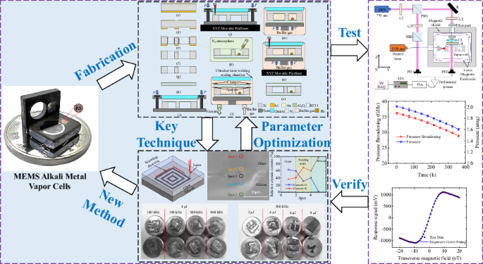
- Gas Leakage Under High-Temperature Constraints: Even with precise bonding, gas leakage can occur particularly during prolonged high-temperature conditions. Studies on ultrafast laser welded MEMS vapor cells demonstrated leakage rates comparable to anodic bonding, albeit with some room for improvement.
As a case in point, experiments have shown that after heating vapor cells to about 150°C under vacuum for 15 days, the leakage rate was maintained at approximately 7.40 × 10⁻¹⁰ Pa·m³/s – a value that sits well within acceptable limits for high-performance quantum sensors. This highlights how proper fabrication techniques, combined with ultrafast laser welding, can overcome the nerve-racking challenge of maintaining long-term sealing integrity.
Economic and Industrial Benefits: Why Small Business and High-Tech Industries Are Taking Note
The attractiveness of ultrafast laser welding as a fabrication technique is not limited to its scientific merits; its economic and industrial implications make it a must-have process in a variety of sectors. With the automotive, electric vehicle, and industrial manufacturing sectors increasingly seeking miniaturized, high-performance sensors, the ability to produce MEMS vapor cells efficiently and reliably is key.
Some benefits that have caught the attention of small business owners and industry leaders include:
- Improved Production Efficiency: With optimized parameters, the process can achieve production rates comparable to or better than anodic bonding methods. This means that manufacturers can produce batches of vapor cells in two hours on 4-inch wafers, significantly reducing production bottlenecks.
- Lower Complexity in Equipment Setup: Unlike methods that require cumbersome high-temperature ovens and high voltage setups, ultrafast laser welding equipment is more compact and easier to integrate into existing manufacturing lines.
- Enhanced Device Longevity: The controlled heating process minimizes degradation of sensitive components and prevents the evaporation of alkali metals, translating to devices with a longer operational life span.
- Competitive Edge in the Quantum Sensor Market: High hermeticity and reduced processing stress offer improved device performance – a critical factor as quantum sensors become increasingly important in precise navigation, automotive systems, and electric vehicle applications.
For companies that are trying to find their way through adopting new techniques, these benefits underscore the potential of ultrafast laser welding to not only simplify manufacturing but also to boost the performance and reliability of MEMS devices. With ongoing advancements and cost reductions, this technology is set to level the playing field even for smaller players competing with larger industrial giants.
Overcoming Overwhelming Technical Challenges: Fine-Tuning the Process
The adoption of ultrafast laser welding in the fabrication of MEMS vapor cells is not without its own set of hurdles. Manufacturers must contend with several subtle parts – including the specific effects of gas absorption, micro-lensing near the focal point, and thermal accumulation – to ensure a robust and leak-free weld.
Some of the most significant technical steps that need to be optimized include:
- Adjusting Pulse Energy and Repetition Frequency: Finding the balance between a pulse energy that is too low (which might create holes or a weak bond) and one too high (risking damage via glass ablation) is a delicate endeavor. The sweet spot identified so far has been around 4 μJ with a repetition frequency of approximately 500 kHz.
- Managing Heat Accumulation: At higher repetition frequencies, increased heat accumulation can lead to micro-lensing effects that reduce the size of the welding seam. Manufacturers have to take a closer look at managing thermal effects to avoid disturbing the delicate balance in the welded area.
- Optimizing the Welding Geometry: The design of the welding path – sometimes including pre-sealing of the vapor cell edges to avoid undue stress on the chamber’s sidewalls – is a critical factor ensuring the integrity of the final product. The edge pre-sealing minimizes the effects of pressure fluctuations during welding and gas charging steps.
Table 2 below summarizes a few common objectives and the corresponding process tweaks that can help achieve them:
| Objective | Potential Process Tweak |
|---|---|
| Prevent weak bonding | Optimize pulse energy and ensure optical contact between silicon and glass |
| Minimize glass ablation | Limit the single pulse energy and monitor nonlinear absorption effects |
| Reduce thermal build-up | Set the repetition frequency to balance heat accumulation with welding seam quality |
| Achieve high hermeticity | Use precise clamping platforms and pre-sealing methods for reliable optical contact |
For many small-scale engineers and business owners, these process tweaks might seem intimidating at first. However, by diving deep into the scientific principles – such as the Fokker–Planck model and two-temperature considerations that underlie the energy transfer mechanisms in ultrafast laser welding – one can figure a path to mastery over these processes. The key lies in systematically testing and iterating on the parameters until the optimal balance is reached.
Maintaining Hermetic Sealing Under High-Temperature Conditions
One of the most critical aspects of MEMS vapor cells is ensuring that the seal remains robust under operational conditions, which often include high temperatures. In applications such as single-beam SERF magnetometers, even slight leaks or variations in buffer gas pressure can alter sensor performance in subtle but significant ways.
Researchers have investigated the behavior of sealed cells under high-temperature vacuum conditions – a test that mimics the nerve-wracking environments in which these sensors must operate in real life. For instance, vapor cells filled with helium as a buffer gas have been held at 150°C for extended periods (up to 15 days) while monitoring changes in pressure broadening.
Key findings include:
- The measured pressure broadening decreased slightly during extended high-temperature exposure, indicating a slow leakage process.
- The effective helium leakage rate was around 7.40 × 10⁻¹⁰ Pa·m³/s, which is comparable to the leakage rates achieved with anodic bonding using traditional methods.
- The use of thin Al₂O₃ coatings on the glass substrate further slowed the leakage process, highlighting the importance of material choices in the overall design.
This detailed information is crucial as it demonstrates that ultrafast laser welding, when executed correctly, yields high-hermeticity bonds that are not easily compromised even in challenging thermal environments. The controlled and confined heating makes it easier to sort out issues related to gas permeation and ensures that the device remains stable over its operational life.
Application Potential in Single-Beam SERF Magnetometers and Beyond
The ultimate aim of fabricating high-quality MEMS vapor cells is to integrate them into advanced sensor systems – such as single-beam spin-exchange relaxation free (SERF) magnetometers. These devices are essential in measuring extremely small magnetic fields with high sensitivity. Ultrafast laser welding not only meets the criteria for a strong, leak-free bond but also helps in maintaining the integrity of the sensitive components housed within the vapor cell.
In a typical single-beam SERF magnetometer:
- A distributed feedback laser is used to generate a beam that heats and polarizes the alkali metal within the vapor cell.
- The polarization process is monitored using carefully designed optical paths that lead to the detection system, which is calibrated to sense even very minute changes in magnetic fields.
- The well-sealed vapor cell guarantees that the buffer gas pressure remains stable, thereby ensuring the sensor produces accurate measurements – a key requirement in applications such as biomagnetic sensing and navigation.
Recent experimental setups have demonstrated magnetometer sensitivities as low as 40 fT/Hz1/2, showcasing how effective fabrication methods contribute to the overall performance of the device. Such sensitivities are super important in fields like medical diagnostics, where even slight magnetic disturbances can signal critical underlying conditions.
Environmental Considerations and Long-Term Stability
Another layer of interest when discussing MEMS vapor cell fabrication involves the environmental stability of the sealed cells. With increasing demands on sensor longevity and reliability – particularly in automotive and aerospace applications – the long-term performance of these devices is under close scrutiny.
Questions such as how the sealing method copes with mechanical shocks, thermal cycling, and even gas permeation over time are key to determining the commercial viability of the technology. Early indicators suggest that ultrafast laser welding could be less loaded with issues compared to traditional methods, as it minimizes the contact area exposed to potential contaminants and defects.
For example, while anodic bonding often requires rigorous pre-cleaning and de-gassing of wafers, ultrafast laser welding, due to its targeted energy delivery, appears to be more forgiving with respect to minor surface contaminations. Furthermore, the incorporation of anti-relaxation coatings, such as octadecyltrichlorosilane (OTS), is made more feasible due to the lower thermal stresses involved. With a maximum sidewall temperature recorded at about 90°C – well below the failure threshold for such coatings – manufacturers can be more confident that the sensor’s performance will remain robust over time.
Opportunities for R&D and Future Process Improvements
While the experimental evidence supporting ultrafast laser welding is promising, there remains significant room for further research and development. Both academic and industrial researchers are now actively dating the process, trying to refine the technique and increase its adoption rate in real-world manufacturing.
Areas that merit further investigation include:
- Welding Speed and Throughput Optimization: Current processes achieve production on 4-inch wafers in about 2 hours. However, research has shown that with advanced equipment, speeds as high as 2 m/s can be achieved. This would dramatically change production economics for small business manufacturers.
- Material Interactions at the Interface: More work is needed to understand the subtle details of how silicon and glass mix during the melting process, particularly concerning elemental distribution and chemical diffusion. Such knowledge can help improve bond strength and reduce weak points.
- Integration with Anti-Relaxation Coatings: As the industry moves toward even miniaturized vapor cells, ensuring that protective anti-relaxation coatings survive the welding process will be key. The lower thermal footprint of ultrafast laser welding is promising, but further tests will solidify this advantage.
- Improved Clamping and Optical Contact Methods: Ensuring a perfect optical contact between the wafers before welding is critical. Enhanced clamping platforms that can offer fine control over the contact parameters may further improve yield and repeatability.
These research paths not only support technological improvements but also hold economic promise. Small businesses can leverage these innovations to gain a competitive edge by reducing manufacturing costs, boosting product reliability, and ultimately enhancing market adoption of MEMS-based quantum sensors.
Implications for the Future of Quantum Sensing and Industrial Manufacturing
There is a growing awareness across various industries that the next wave of innovation in sensor technology – particularly quantum sensors – hinges on the durability and performance of minute components such as MEMS vapor cells. Whether in the automotive sector where advanced navigation systems need to function reliably under heavy stress, or in electric vehicles where precision sensing can lead to better energy management and safety systems, the role of robust fabrication methods is pivotal.
Ultrafast laser welding is not just a novel process for academic labs; it is poised to become a game changer in the broader market. With its ability to produce high hermeticity bonds under controlled, localized thermal conditions, it opens the door for more reliable, sensitive, and long-lasting sensors. For industrial manufacturers, this means that operational deadlines may be shortened and overall device performance improved, with fewer repair recalls or quality issues over a product’s lifetime.
Small business owners, in particular, stand to benefit. The reduced need for large-scale, expensive apparatus – combined with better production throughput – means that even startups in the quantum sensor space can now compete on price and performance. In this context, ultrafast laser welding reflects not only a technical advance but also a strategic business opportunity.
Sorting Out the Fine Points and Hidden Complexities
For those interested in the technical side of the process, there are several fine points and little twists that merit a closer look. One of the most interesting aspects is the energy coupling mechanism that drives the welding process. By applying rigorous theoretical models – such as the Fokker–Planck equation and two-temperature model – researchers have been able to pinpoint how free electron dynamics and lattice heating yield a high-strength bond between the silicon and glass substrates.
The hidden complexities, however, are not just academic. They manifest in practical challenges such as the fine-tuning of laser parameters and in the precise management of the welding path. For example, a slightly off-target laser focal position might lead to micro-lensing effects near the welding seam or uneven heat distribution. These are issues that, while seemingly minor, have significant repercussions for the long-term stability of the vapor cells.
Fortunately, modern manufacturing techniques allow for rapid testing and calibration of multiple parameters simultaneously. Advanced sensors and feedback mechanisms can help manufacturers figure a path through these subtle details, eventually leading to a process that is both highly repeatable and robust in mass production environments.
Steering Through Regulatory and Quality Assurance Maze
Quality assurance is, of course, an essential part of any manufacturing process – and it is no different when it comes to MEMS vapor cell fabrication. Given the critical nature of these components in precision applications, ensuring that each cell meets strict leakage and hermeticity standards is super important.
For instance, guidelines such as the GJB 548B-2005 standard on leakage rates set strict limits on permissible leakage levels. In the studies involving ultrafast laser welding, comprehensive tests including prolonged high-temperature vacuum exposures have demonstrated that the leakage remains below these thresholds. Such testing is imperative in reassuring both regulators and end-users that the technology is not only innovative but also reliable.
From an operational standpoint, the integration of real-time diagnostic tools during fabrication – including residual gas analyzers, pressure gauges, and high-resolution microscopic imaging – provides continuous feedback. This helps manufacturers quickly identify and address any confusing bits or subtle issues that could compromise the product’s quality.
Making Your Way Through Market Trends and Technological Adoption
The broader market for MEMS-based sensors and quantum devices is evolving rapidly. With a growing interest from sectors such as industrial manufacturing, automotive, and electric vehicles, manufacturers are increasingly under pressure to adopt new technologies that enhance performance while reducing production costs.
In this regard, ultrafast laser welding stands out as a technique that is both innovative and commercially viable. The following bullet list summarizes key market trends that are driving the adoption of advanced fabrication methods:
- Demand for Miniaturized Sensors: Higher device density and improved performance in consumer electronics, automotive sensors, and industrial measurement systems.
- Cost-Effective Production: Reduced processing times and lower thermal budgets lead to lower operational costs and higher production yields.
- Increased Precision and Stability: The drive for devices with long operational lifespans and minimal performance drift over time.
- Eco-friendly Manufacturing: A shift towards processes that generate fewer contaminants and require less energy-intensive equipment.
- Scalability for Start-ups: Technologies that are accessible even to small businesses with limited capital investment.
Market leaders who steer through these trends by integrating advanced techniques like ultrafast laser welding into their production lines are likely to set new benchmarks in sensor performance and manufacturing efficiency. This not only helps in capturing larger market shares but also positions them as innovators in their respective niches.
Final Thoughts: The Road Ahead for MEMS Vapor Cell Technology
In summary, the adoption of ultrafast laser welding in the fabrication of MEMS alkali metal vapor cells represents an exciting turning point. With a robust body of research supporting its benefits – including superior hermeticity, reduced thermal damage, and high production efficiency – this technique is proving to be a promising alternative to traditional anodic bonding methods.
Although there remain some intimidating technical challenges – such as optimizing pulse energy, managing thermal accumulation, and ensuring long-term gas integrity – the overall progress is very encouraging. With continuous R&D, improved clamping platforms, and advanced diagnostic tools, many of these tricky parts and tangled issues can be gradually sorted out, paving the way for widespread industrial adoption.
For small business owners and industrial manufacturers alike, the ability to produce robust, high-performance vapor cells quickly and cost-effectively could well be the key to driving the next wave of innovation in quantum sensor technology. The potential impact on sectors ranging from precision automotive sensors to high-end medical devices is enormous.
In essence, ultrafast laser welding is not merely an alternative fabrication method – it represents a new paradigm that simplifies the challenging aspects of MEMS vapor cell production. As these techniques become more refined, the technology is likely to see widespread adoption, resulting in a new generation of quantum sensors that are both reliable and economically competitive.
As the field continues to evolve, it will be fascinating to observe how these innovations further influence market dynamics and industrial practices. Whether you are an engineer, a small business owner, or a decision-maker in a large manufacturing enterprise, the message is clear: staying abreast of these advancements is critical, and ultrafast laser welding is poised to play a super important role in shaping the future of quantum sensor technology.
Ultimately, the ongoing dialogue between academic research and industrial application is steering the industry toward new heights. By embracing ultrafast laser welding and its associated benefits, stakeholders can not only overcome the nerve-wracking challenges of traditional methods but also set a new standard for precision, efficiency, and long-term device stability in the fast-growing field of MEMS vapor cell technology.
Originally Post From https://www.nature.com/articles/s41378-025-00976-6
Read more about this topic at
From concept to industry: Ultrafast laser welding
Improved Femtosecond Laser Welding of Nonoptical Contact …